lunes, 15 de febrero de 2010

RF-MEMS Switches for Reconfigurable

RF-MEMS Switches for Reconfigurable
Integrated Circuits
Abstract — This paper deals with a relatively new area of radio-frequency (RF) technology based on microelectromechanical systems (MEMS). RF MEMS provides a class of new devices and components which display superior high-frequency performance relative to conventional (usually semiconductor) devices, and which enable new system capabilities. In addition, MEMS devices are designed and fabricated by techniques similar to those of very large-scale integration, and can be manufactured by traditional batch-processing methods. In this paper, the only device addressed is the electrostatic microswitch—perhaps the paradigm RF-MEMS device. Through its superior performance characteristics, the microswitch is being developed in a number of existing circuits and systems, including radio front-ends, capacitor banks, and time-delay networks. The superior performance combined with ultra-low-power dissipation and large-scale integration should enable new system functionality as well. Two possibilities addressed here are quasi-optical beam steering and electrically reconfigurable antennas.

 I.  INTRODUCTION

The 1990's have brought a profound change in radio-frequency (RF) technology driven largely by economic Tand geopolitical events. On one hand, the wind-down of the cold war has reduced the need for advanced RF systems, particularly sensors; on the other hand, the dawning of the information age has created a heightened interest and world-wide market for  communications  systems and networking of voice and data alike.The transition of RF technology from one era to the other has been both challenging and opportunistic. For the RF systems engineers, it has meant a shift of thinking from large centralized systems to smaller distributed systems. Along with this shift has come a change from long-range systems, having large RF transmit power, to shorter range systems, having relatively modest RF power. In many cases, the new smaller  systems must be mobile or hand-held. The paradigm for these new systems is the cellular wireless network consisting of a single powerful base station feeding a local cell of hand sets acting like individual terminals or nodes of the network. The popular digital cellular and personal communications service (PCS) bands around 0.9 and 1.9 GHz, respectively, comprise much of the frequency spectrum being used for cellular purposes.
 
For technology engineers, the transition has been no less challenging. The premium devices and components formerly required to construct powerful centralized systems are no longer required or can no longer be afforded in many new distributed systems coming on line today. Instead, there is an emphasis on more affordable and integrable technology, which allows a greater degree of RF functionality per unit volume, even if at a lower level of performance than obtained with the former technologies. This has spawned widespread research and development of silicon-based RF integrated circuits (RFIC's), including deep-submicrometer Si CMOS and SiGe heterojunction bipolar transistors (HBT's). Taking advantage of the inherent manufacturability of Si very large-scale integration (VLSI), RFIC technology has found unique circuit and subsystem architectures well outside the traditional digital design. One example of this is the "RF system-on-a-chip," such as the family of integrated circuits (IC's) now commercially available for global positioning receivers.
This paper deals with another technology that has emerged in recent years with a comparable level of interest and more rapid development than RFIC's. The technology is the design and fabrication of microelectromechanical systems (MEMS) for RF circuits (RF MEMS). In some ways, MEMS represents the new revolution in microelectronics. It is similar to VLSI circuits in that it allows the execution of complex functions on a size scale orders of magnitude lower and at far less power than discrete circuits. However, MEMS enables this miniaturization on a class of sensors and transducers that traditionally were constructed on the model of a large, often cumbersome transducer or sensor coupled to a highly integrated VLSI readout circuit or processor. A good example of this is the MEMS accelerometer, now one of the largest single MEMS application through its incorporation in air bags [1]. At the same time, MEMS leverages VLSI through the use of common design and batch processing methodologies and tools. It is this commonality with VLSI that has been credited to a large extent for the rapid dissemination of MEMS into the commercial marketplace.
It is important to realize up front that RF MEMS does not necessarily imply that the micromechanical system is operating at RF frequencies. As will be discussed briefly, in the largest class of RF MEMS devices and components, the microelectromechanical operation is used simply for the actuation or adjustment of a separate RF device or component, such as a variable capacitor. In many of these devices, a key advantage of the MEMS devices compared to traditional semiconductor devices is electromechanical isolation. By this, we mean that the  RF circuit does not leak or couple significantly to the actuation circuit. A second advantage is power consumption. Many of the RF MEMS devices under development carry out electromechanical coupling electrostatically through air (or vacuum). Hence, the power consumption comes from dynamic current flowing to the MEMS only when actuation is occurring. However, the implementation of RF MEMS does not come with  impunity. Due to the mechanical actuation, they are inherently slower than electronic switches. The electromechanical actuation time is typically many microseconds or greater, which is substantially longer than typical electrical time constants in semiconductor devices. In addition, RF MEMS devices can exhibit the phenomenon of "stiction," whereby parts of the device can bonded together upon physical contact. Each of these issues will be discussed further.
II.  MEMS AND  MICROMACHINING

 According to a recent definition, a MEMS is a miniature device or an array of devices combining electrical and mechanical components and fabricated with IC batch-processing techniques [2]. Critical to this definition is that MEMS has both device and fabrication aspects. There are several MEMS fabrication techniques currently in widespread use, including bulk micromachining, surface micromachining, fusion bonding, and LIGA, which is a composite fabrication procedure of lithography, electroforming, and molding. The most important technique for RF MEMS is surface micromachining. In short, surface micromachining consists of the deposition and lithographic patterning of various thin films, usually on Si substrates. Generally, the intent is to make one or more of the ("release") films freestanding over a selected part of the substrate, thereby able to undergo the mechanical motion or actuation  characteristic of all MEMS. This is done by depositing a "sacrificial" film (or films) below the released one(s), which is removed in the last steps of the process by selective etchants. The  variety of materials for the release and sacrificial layers is great, including many metals (Au, Al, etc.), ceramics (SiO and Si N ), and plastics (photoresist, polymethyl methacrylate (PMMA), etc.). Depending on the details of the MEMS process and the other materials in the thin-film stack, the release and sacrificial layers can be deposited by evaporation, sputtering, electrodeposition, or other methods.
Surface micromachining has been used for a long time, dating back to MEMS work of the 1960's at Westinghouse. A breakthrough in surface micromachining has come in the form of dry etching, particularly reactive-ion etching (RIE). By mixing reactive chemicals in a plasma discharge  and adding a semiconductor wafer with thin films deposited on top, select materials on the surface can be etched away at useful high rates and with high levels of material selectivity. For example, chlorine-bearing compounds in a high-density plasma can yield nearly isotropic silicon etching with a selectivity of silicon-to-SiO  of better than 100 : 1. By the same token, low-pressure plasma etching [e.g., inductively coupled plasma (ICP)] allows independent control of the ion density and energy.
Neyker Stewart Zambrano
CRF

Monolithic Microwave Integrated Circuits

Monolithic Microwave Integrated Circuits

Monolithic microwave integrated circuits (MMICs) and similar devices are used in a wide variety of receivers. These devices may be very wideband or relatively narrowband. Very wideband amplifiers have a bandpass (frequency response) of several hundred megahertz or more, typically ranging from sub-VLF to the low end of the microwave spectrum. An example might be a range of 100 kHz to 1000 MHz (i.e.,  1 GHz), although somewhat narrower ranges  are more common. These circuits have a variety of practical uses: receiver preamplifiers, signal generator output amplifiers, buffer amplifiers in RF instrument circuits, cable television line amplifiers, and many others in communications and instrumentation.

One reason why very wideband amplifiers are rarer than narrowband amplifier circuits is that they were difficult to design and build until the advent of monolithic microwave integrated circuit devices. Several factors contribute to the difficulty of designing and building very wideband amplifiers. For example, too many stray capacitances and inductances are in a typical circuit layout, and these form resonances and filters that distort the frequency response characteristic. Also, circuit resistances combine with the capacitances to effectively form low-pass filters that roll off the frequency response at higher frequencies, sometimes drastically.  If the RC phase shift of the circuit resistances and capacitances is 180º at a frequency where the amplifier gain is ≥1 (and in very wideband circuits that is likely) and the amplifier is an inverting type (producing an inherent 180º phase shift), then the total end-to-end phase shift is 360º—the criteria for self-oscillation.

If you have ever tried to build a very wideband amplifier, it likely was a very frustrating experience. Until now. New, low-cost devices, called silicon MMICs, make it possible to design and build amplifiers that cover the spectrum from near DC to about 2000 MHz,  using seven or fewer components. These devices offer 13–30 dB of gain and produce output power levels up to 40 mW (+16 dBm). Noise figures range from 3.5 to 7 dB. In this chapter, we use the MAR-X series of MMICs by Mini-Circuits Laboratories as representative.

The only connections are RF input, RF output, and two ground connections. The use of dual ground connections distributes the grounding, reducing overall inductance and thereby improving the ground connection. Direct current power is applied to the output terminal  through an external network. But more on that shortly.

Although an IC, the device looks very much like a small UHF/microwave transistor. The body  is made of plastic and the leads are wide metal strips (rather than wire) to reduce the stray inductance that narrower wire leads would exhibit. These devices are small enough that handling can be difficult; I found that hand forceps (tweezers) were necessary to position the device on a prototype printed circuit board. A magnifying glass or jeweler's eye loupe is not out of order for those with poor close-in eyesight. A color dot and a beveled tip on one lead are the  keys that identify pin 1 (the  RF input connection). When viewed from above, pin numbering  (1,  2,  3,  4) proceeds counter-clockwise from the keyed pin.
INTERNAL CIRCUITRY

The MAR-X series of devices inherently matches 50 Ω input and output impedances without external impedance transformation circuitry, making it an excellent choice for general RF applications. These devices are silicon bipolar monolithic ICs in a two-transistor Darlington amplifier configuration. Because of the Darlington connection, the MAR-X devices act like transistors with very high gain. Because the transistors are biased internal to the MAR-X package, the overall gains typically are 13–33 dB, depending on the device selected and operating frequency. No external bias or emitter bias resistors are needed, although a collector load resistor to V+ is used.
Neyker Stewart Zambrano
CRF

RF/MICROWAVE GLOSSARY

RF/Microwave Glossary
Albaloy: A plating finish comprised primarily of copper, tin and zinc which provides good electrical performance, but unlike silver, albaloy is highly resistant to tarnish.  Being non-magnetic, it also provides excellent passive intermodulation (PIM) performance comparable to silver.

Amplitude Balance: The maximum peak-to-peak amplitude difference (in dB) between the output ports of a power divider or hybrid coupler over the specified frequency range.

Attenuation Accuracy: The amount of variation in magnitude from the nominal value across the entire frequency band.
Attenuator: A passive device or network that absorbs part of the input signal and transmits the remainder with minimal distortion. Attenuators are used to extend the dynamic range of devices such as power meters and amplifiers, reduce signal levels to detectors, match circuits and are used daily in lab applications to aid in product design. Attenuators are also used to balance out transmission lines that otherwise would have unequal signal levels.

Base Station: A fixed transmitter/receiver with which a mobile radio transceiver establishes a connection link to gain access to the public-switched telephone network.

Bias Tees: A passive device used in applications to inject/remove DC voltages in RF circuits without affecting the RF signal through the main transmission path.  Ideal for remote powering of bi-directional amplifiers (BDAs), repeaters and tower top amplifiers (TTAs) by BTS control modules. 
Circulator: A three-port ferromagnetic passive device used to control the direction of signal flow in an RF circuit.

Coaxial: A transmission line in which one conductor completely surrounds the other, the two being coaxial and separated by a continuous dielectric such as air or PTFE.

CW – (Continuous Wave): Signal of constant amplitude.  Used to differentiate between the performance of a microwave component for continuous power level vs. pulsed signals.

dB – (Decibel): A unit of gain equal to ten times the common logarithm of the ratio of two power levels or 20 times the common logarithm of the ratio between two voltages.

dBc: Decibel related to the signal of a carrier.  Passive intermodulation distortion is typically stated in dBc which takes into consideration the 43 dBm carrier tones.

dBm: Decibels related to 1mW – the standard unit of power level used in the microwave industry.  Example: 0 dBm = 1mw,  +10 dBm = 10mw,  +20dBm = 100mw, etc.

DC Block: An in-line device primarily used in applications to block DC voltages in RF circuits without affecting the RF signal through the main transmission path.  The three basic types are:
Inner – Blocks DC voltages on inner conductor only
Outer – Blocks DC voltages on outer conductor only
Inner/Outer – Blocks DC voltages on both conductors

Directional Coupler: A passive device used for sampling incident and reflected microwave power conveniently and accurately with minimal disturbance to the transmission line. Some general applications for directional couplers include line monitoring, power measurements and load source isolators.

Directivity: A measurement of the desired signal strength to the undesired signal strength.  Determined by taking the value of isolation and subtracting the specified coupling (including all variations).  Directivity is a measure of how good the couplers performance is (similar to the Q factor of a coil).

EMI – (Electromagnetic Interference):  Unintentional interfering signals generated within or external to electronic equipment.  Typical sources could be power line transients and electromechanical switching equipment.
Frequency Range: The minimum and maximum frequencies between which the specified component will meet all guaranteed specification.
Frequency Sensitivity: The maximum peak-to-peak variation in coupling (in dB) of a directional or hybrid coupler over the specified frequency range.  Also referred to as "flatness".
GHz - (Gigahertz): A unit of frequency measure equal to 1000 MHz (Megahertz) or a billion hertz.
Hybrid Coupler: A passive four-port device that is used either to equally split an input signal with a resultant 90° phase shift between output signals or to combine two signals while maintaining high isolation between them.
Impedance: Resistance to alternating current.  Most RF and microwave systems are designed to operate with a characteristic impedance of 50 ohms.
Input VSWR: Minimum voltage standing wave ratio of a power divider at the input (sum) port over the specified frequency range with all other ports terminated in 50 ohm loads.
Insertion Loss: The change in load power due to the insertion of a particular device into a transmission system.
Iridite: A chemical film (typically clear or yellow in color) which provides a barrier medium to prevent corrosion on aluminum surfaces and enhance adhesion of subsequent coatings such as paints and primers.
Isolation:  A unit of measure (in dB) that states the separation of signal levels on adjacent ports of a device.  The greater the isolation value, less interference from a signal on one port is present at the other.
Isolator:  A two-port ferromagnetic passive device which is used to control the direction of signal flow and utilizes an internal resistor.  Typically used to protect other RF components from excessive signal reflection.
MHz - (Megahertz): A unit of frequency measure equal to 1000 kHz (Kilohertz) or a million hertz.
Microstrip – (Microstripline): A transmission line consisting of a metalized strip and solid ground plane metallization separated by a thin, solid dielectric.  Microstrip is a popular material above 400 MHz and below 6 GHz because it permits accurate fabrication of transmission lines on ceramic or PC board substrates.  Higher frequencies or broadband devices tend to favor stripline technology.
MTBF – (Mean Time Between Failure): The mean (average) time between failures of a component and is often attributed to the "useful life" of the materials used to assemble the device.  MTBF assumes that the component can be "renewed" or fixed after each failure and returned to service immediately after failure.
Non-Coherent Signals: The limiting factor for most Wilkinson power dividers used as combiners is power dissipation. When input signals are out of phase, non-coherent or have amplitude unbalance this causes a cancellation across the isolation resistors resulting in power dissipation.  Since these devices are most commonly used as dividers, typical industry designs utilize low power alumina surface mount resistor chips on a thermally insulative circuit board. However, maximum input for combining non-coherent signals on adjacent ports is:
(Rated input power of divider * 5%) / "N" # of input channelsIf the rated power is exceeded, the chip resistors will heat up and degrade resulting in loss of port-to-port isolation and VSWR.

Output VSWR: Minimum voltage standing wave ratio of a power divider at any output port over the specified frequency range with all other ports terminated in 50 ohm loads.
Passivation: The formation of an insulated layer directly over a metal to protect the surface from contaminants, moisture or particles.
Phase Balance: The maximum peak-to-peak phase difference (in degrees) between the output ports of a power divider over the specified frequency range.
PIM (Passive Intermodulation): Passive Intermodulation (PIM) occurs when two or more signals are present in a passive device (cable, connector, coupler, etc.) that exhibits a nonlinear response. The nonlinearity is typically caused by dissimilar metals or dirty/loose interconnects.   Nonlinearity is typically not troublesome at low input signal levels, but if PIM is generated from a high power transmitter path to an adjacent receiver channel, desensitization will occur.   A common PIM specification is typically -110 dBc or greater.
Power (Average): The maximum amount of mean (average) power of a modulated/pulsed signal a given component can dissipate at ambient temperature without degradation in performance.
Power (Peak): Instantaneous power a given component can dissipate for a percentage of the duty cycle (typically 2%) without degradation in performance.
PTFE (PolyTetraFluoroEthylene): Used as an insulator in RF and microwave coaxial connectors because of its low & stable dielectric constant and loss factor over a wide temperature and frequency range.
Reactive Splitter:  A broadband passive network that equally divides power applied to the input ports between any particular number of output ports without substantially affecting the phase relationship or causing distortion.  Reactive splitters differ from Wilkinson power dividers as they provide no isolation between adjacent ports.  Therefore, power entering any output of a reactive splitter will divide evenly between the adjacent and input ports.
Return Loss: When expressed in dB is the ratio of reflected power to incident power.  It is a measure of the amount of reflected power on a transmission line when it is terminated or connected to any passive or active device.  Once it is measured, it can be converted by equation to reflection coefficient which can be converted to VSWR.
RF – (Radio Frequency): Generally referring to any frequency at which the radiation of electromagnetic energy is possible typically above 50 MHz.  Above 1000 MHz and up is considered microwave.
RF Leakage: The amount of energy which "leaks" or radiates from a connector and/or device.  Typically tested at one frequency and expressed in dB.  Very large negative values indicate that the device does not radiate much energy.
RoHS: (Restriction of Hazardous Substances) Directive adopted by the European Union in February 2003 with the specified limits for the following elements in the manufacture of various types of electronic and electrical equipment:
Lead (Pb) < 0.1%
Mercury (Hg) < 0.1%
Cadmium (Cd) < 0.01%
Hexavalent Chromium (CrVI) < 0.1%
Polybrominated Biphenyls (PBB) < 0.1%
Polybrominated Diphenyl Esters (PBDE) < 0.1%
Stripline: A transmission line consisting of a conductor above or between extended conducting surfaces.  Higher frequencies or broadband devices tend to favor stripline technology.
Termination (RF Loads): Used at the end of a transmission line designed to absorb RF power with very little reflection, effectively terminating the line or port in its characteristic impedance. Terminations are used in a wide variety of measurement systems; any port of a multi-port microwave device that is not involved in the measurement should be terminated in its characteristic impedance in order to ensure an accurate measurement.
Temperature: The minimum and maximum ambient temperatures a given component can operate at and still meet all guaranteed specifications unless otherwise noted.
Torque:  Recommended mating torque for industry standard connectors:
SMA - 7 to 10 in-lbs
Type-N – 12 to 15 in-lbs
TNC – 12 to 15 in-lbs
7/16 DIN – 220 to 300 in-lbs
Transmission Line: The conductive connections between circuit elements which carry signal power.  Wire, coaxial cable, microstrip and stripline traces and waveguide are common examples.
VSWR – (Voltage Standing Wave Ratio): The ratio of the incident signal compared to the reflected signal in a transmission line.  VSWR cannot be directly measured, so a return loss measurement (expressed in dB) is taken of reflected power to incident power.  Once it is measured, it can be converted by equation to reflection coefficient which can be converted to VSWR.
Wilkinson Power Divider: A passive device that equally splits an input signal to each output or combines signals to a common port.  Wilkinson power divider differ from reactive splitters as the output ports are isolated, so signals entering one of the output ports will not interfere with signals on the adjacent port.  The limiting factor for Wilkinson power dividers used as combiners is power dissipation. When input signals are out of phase, non-coherent or have amplitude unbalance this causes a cancellation across the isolation resistors resulting in power dissipation.
Neyker Stewart Zambrano
CRF

TRFIC and Microwave Circuits

Frequency divider design strategies
Typically, in frequency divider design, the trade offs are around the maximum operating frequency, power consumption, number of transistors needed and flexibility. Depending on the specific application the frequency divider is used, analog or digital approaches may be adopted. This paper will cover the fundamentals of both approaches.

The frequency divider is an important building block in today's RFIC and microwave circuits because it is an integral part of the phase-locked loop (PLL) circuit. In a typical PLL loop, the output of the voltage-controlled oscillator (VCO) is divided down by the frequency divider to a frequency the temperature-compensated crystal oscillator (TCXO) operates (typically from 10 MHz to 30 MHz). The divided signal and TCXO are fed into the phase detector for comparison. The output phase difference is used to adjust the VCO output frequency. The frequency divider is also widely used to generate a precision I/Q signal if the input signal has a 50% duty cycle, for the modern in-phase and quadrature (I/Q) modulator or demodulator. For the signal with duty cycle other than 50%, an additional divide- by-2 can be used to generate the 50% duty cycle. Compared with the traditional resistor and capacitor (RC) quadrature generation, the frequency divider approach is easier to implement, is lower power and offers smaller phase imbalance.

Digital logic approaches

Since the PLL is part of the RF circuit, one would think the frequency divider should be analyzed by the analog circuit theory. But it turns out the most widely used approach is based on the digital logic gate. The RF analog engineer typically puts on the digital logic hat for a minute when analyzing the frequency divider. It will be much easier to understand and analyze the digital approach in the digital domain and the analog approach in the analog domain. Within the digital domain, the design strategy can be further divided into two categories: static logic and dynamic logic.
The static implementation is the most popular approach. The memory cell is a true bistable circuit, unlike the parasitic capacitor used in the dynamic approach. One standard design is the divider by 2 cell. In today's design software, it is treated as a standard digital cell. There are many names for circuits, such as a Johnson divider, toggle switch, complementary metal oxide semiconductor (CMOS) prescaler, emitter couple logic (ECL) and a source couple logic (SCL). When it is implemented in CMOS, it is called SCL. When it is implemented in a bipolar process, it is logically called ECL. For this illustration, CMOS implementation (SCL) is used.
The first look at this design might be intimidating for an RF design engineer. It doesn't look like an RF circuit with the exception of the differential amplifier and cross-coupled negative channel field effect transistor (nFET) of a VCO. Treating it as a pure RF circuit will make it much harder to understand. However, once analyzed in the digital domain, the answer will be clear. Before the detailed discussion of this cback to the input port D. The same clock is used to drive both level-triggered DFF with opposite logic. The reason for the inverter is to make an edge-triggered DFF out of the two level-triggered DFF. The first DFF is commonly called the master DFF and the second one is normally referred to as the slave DFF. Either master DFF or slave DFF is activated in each clock cycle, not both DFF at the same timeircuit, some of the fundamental digital logic theory should be reviewed.
The theory of operation is straightforward. It is essentially an edge-triggered master/slave D flip-flop (DFF). The inverted output is fed back to the input port D. The same clock is used to drive both level- triggered DFF with opposite logic. The reason for the inverter is to make an edge-triggered DFF out of the two level-triggered DFF. The first DFF is commonly called the master DFF and the second one is normally referred to as the slave DFF. Either master DFF or slave DFF is activated in each clock cycle, not both DFF at the same time (because of the inverter between them), each positive input clock cycle is loaded into the DFF. On the next cycle, inverted output again is fed back to the input, which causes the output to toggle. It is why toggle DFF is a more descriptive name for this circuit. The same event repeats for every two input clock cycle. Thus, output frequency is half of the input frequency.
a typical DFF implementation is comprised of cross-coupled NOR gates. Without the inverter, it is recognizable as the familiar SR latch. The next logic step is to take a look at how the SR latch logic is implemented on the transistor level.
Transistor Q2, Q5, Q7 and Q9 form the first NOR gate while Q3, Q6, Q8 and Q10 complete the second NOR gate. It should be obvious that Q2 and Q5 are the pull-down network (PDN) for passing logic 1s and Q7 and Q9 are the pull-up network (PUN) for passing logic 0s. Similarly, the pairs (Q3, Q6) and (Q10, Q8) are the counterparts for the second NOR gate, the circuit is the same circuit used for the edge-triggered DFF SCL implementation with minor modifications. Q2, Q5, Q3 and Q6 are still the same circuit elements rearranged slightly. Q7 and Q8 are still the active loads. Q1 and Q4 act as the input buffer. They also provide the enable function. As discussed earlier, in edge-triggered master-slave DFF, only one DFF is activated at the time. The inverter can be easily implemented by swapping the position of the "+RF" and "-RF" when feeding different DFFs.

Dynamic DFF implementation

In dynamic DFF implementation, there is no dedicated bistable circuitry. The parasitic cap between the node acts as the storage element. It is typically called Clocked CMOS (C2MOS).
This circuit uses a far less number of transistors. The theory ofoperation is simple. Transistors Q1 to Q4 complete essentially a tri-state inverter (INV1). Transistors Q5 to Q9 (INV2) form another inverter. The capacitor in the middle is a model for the parasitic capacitance between the gate. The capacitor's responsibility is to store the signal. Q9 and Q10 make a simple CMOS inverter to complete the feedback path needed for the toggle latch. In the positive clock cycle (RF+), INV1 is on and INV2 is off, so the signal is clocked into the storage capacitor. In the negative clock cycle (RF-), INV1 is off and INV2 is on, the signal is clocked out. There are many different flavors using a similar theory of operation.
The circuit requires the complementary clock input (RF+ and RF-). Sometimes, it is more desirable to drive the frequency divider single ended. The type of logic is called true single-phase clocked (TSPC) logic. It is built on the basic C2MOS. It eliminates the differential drive requirement at the expense of more transistors.
Transistors Q1 to Q6 form the master latches. Transistors Q7 to Q12 form the slave latches. Q13 and Q14 are simply the inverter to complete the feedback path needed in the toggle latch. The master latch is sometimes called double NC2MOS because two NFETs are needed in the PDN. Similarly, the slave latch is sometimes referred to as the double PC2MOS because two PFETs are needed in the PUN. When the clock is high, the master latch is activated while the slave latch is off. The opposite is true when the clock is low.
Comparing the static and dynamic implementation, static logic is faster and more reliable. The dynamic logic uses a far fewer number of transistors and is easier to implement. However, it is slow and it could consume more power because full CMOS swing is needed in certain applications.

Analog approach

The frequency divider with analog approach is also widely used. It tends to be used in the very high frequency millimeter wave range, anywhere from 20 GHz up to 100 GHz. Also, they tend to be in discrete form. The reason for this is the CMOS or BiCMOS process still doesn't have high enough operating frequency range as the more exotic process like pHEMT or heterojunction bipolar transistor (HBT). The analog approach is often called regenerative injection-locked frequency divider (ILFD). Recently, there has been a lot of research to use this technique with CMOS at much lower operating range. However, operating bandwidth is fairly narrow due to the nature of this architecture. In VCO design, one of the key parameters is VCO pulling. Basically, the VCO output frequency will be pulled away if a continuous wave (CW) signal at a different frequency is nearby. VCO pulling is an undesired characteristic, but it is used cleverly to design the ILFD. ILFD is built on this phenomenon by adding a feedback loop, along with a mixer, oscillator or an amplifier with appropriate feedback network and appropriate filters.
From the basic mixer theory, fout=fin-Lo. If fout=Lo, then fin=2*fout. Thus, fin is divided down by half. The active device like an amplifier or a ring oscillator is needed to sustain the oscillation.
The ILFD can be treated as an oscillator operating at fout. The difference is ILFD's output will closely track the input. A good ILFD only oscillates when there is signal injected at the input. The filter is needed to reject all the undesired spurious signals out of the mixer. Otherwise, the ILFD could lock into an undesired frequency output. Since the physical mixer is a non-linear device, it could generate signals at Lo and its harmonics. By carefully controlling which harmonic is generated, higher divider ratio can be achieved. For example, if the Lo's third harmonic is used, then Lo=3*fo. Then fin=3*fo+fo. Thus, the fin=4*fo, a divide-by-4 circuit is accomplished. In an ILFD design, most of the building blocks in a typical receiver are used. Filter, amplifier, oscillator, mixer and feedback network are all rich in theory. There are many good references to cover those topics in details. Some of the references are listed in the reference section. One additional comment with ILFD is on the mixer topology. In the mixer design, harmonics are undesired features. However, as illustrated, the harmonics of the mixer are used to the designer's advantage to design a good ILFD. In the active RFIC mixer implementation, a Gilbert cell double balanced mixer (DBM) is widely used. A well-designed DBM will suppress the even harmonics of the Lo. Then only even divide ratio ILFD can be designed. To design an odd divide ratio ILFD, the even harmonics of the mixer is actually a desired feature. Therefore, a simpler single balanced mixer (SBM) can be used to add more flexibility.

Summary

The frequency divider is an interesting and indispensable building block in RF or microwave circuits. There are two main design approaches: digital logic and analog using injection-lock techniques. The digital logic approach can be further divided as the static DFF and dynamic DFF. Like any other receiver design, design trade offs required depend on the application. In applications from around 40 GHz to 100 GHz, an ILFD is a suitable approach because today's standard CMOS process still doesn't have the bandwidth in that range. From 10 GHz to 40 GHz, successful SCL-type frequency divides have been reported. The power consumption, cost and physical size need to be thoroughly compared to decide if the digital or the analog approach is used. From low GHz to 10 GHz, digital SCL is the working horse in this range. Below the low GHz frequency, a case can be made to use dynamic DFF to reduce the number of the transistors needed, thus the cost and power consumption is reduced as well. In today's RFIC, a programmable divider is often required. The digital approach offers the flexibility and modularity ILFD can't match.
The frequency divider is an actively researched area. There are more clever topologies to be discovered to reduce the size, power consumption, complexity and cost.
Neyker Stewart Zambrano
CRF

RF-Microwave Circuits/Products


RF-Microwave Circuits/Products
fuente:
http:http://www51.honeywell.com/aero/common/documents/myaerospacecatalog-documents/Missiles-Munitions/Accuracy_Attenuators.pdf
http://www.avx.co.il/docs/techinfo/rf_sform.pdf
http://www.anritsu.com.hk/SC/downloads/files/Wirelesscatalog2002.pdf
CRF_Zambrano C. Jaydi D.

RF-Microwave Circuits/Microwave Circuits Prototyping and integration Revolution

Traditional RF and microwave prototyping take weeks to months. MicroWave Cells introduces a completely new and innovative concept to build your desired functions, sub-systems, and systems in just hours and days with a fraction of the traditional prototyping cost. Less cost, better efficiencies. RF and Microwave circuit designs have always been a detailed and tedious process, including many cycles of schematics, layout, PCB fabrication, board mechanics, assembly, and testing. MicroWaveCells offers a fast new RF and Microwave circuit design and prototyping concept (patented) by offering many standard single function PCB cells with MicroWaveCells' unique mechanical cells for use as a single function design or a multi-function sub-system or system design. This rapid and dynamic prototyping concept saves a tremendous amount of time and money compared to the traditional RF/Microwave prototyping cycles.
Single Cells
MicroWaveCells initially offers a total of 132 single PCB cells, which support more than 100 different device footprints and 11 basic mechanical cell parts. PCB cells cover more than thousands of the most commonly used off-the-shelf RF/Microwave devices from most of the key RF/Microwave device vendors. Customers can use these cells to build and test each cell function with corresponding single cell mechanics. Each cell has a standard cell dimension with 20x20mm2. Some cells/functions have more than one single cell dimension, such as the synthesizer cell with a 2x3 cell size and VCO with a 1x2 cell size. The single cell supports most of the key RF functions with common footprints. The cell frequency range covers from DC to 40GHz.


MicroWaveCells also introduces a dynamic, single module concept (patented) based on the standard single cell product line. The single mechanical cell is designed to be connected by sidewalls with covers of the customer's choice. By selecting required sidewalls and covers online, customers can easily make their own modules in minutes.


Dynamic Cells
Unlimited possibilities! This single cell can be extended to any dimension and any shape by using the single cell base and single base joint. The half cell base can be added for the side input or output launch.


The following example shows how a block diagram selects cell PCB and corresponding cell mechanics to build your desired system in days. For bias and control convenience, MicroWaveCells also offers a 1x5 DC management cell. The output microwave filter is a customized 1x2 cell size filter.


Array Cells

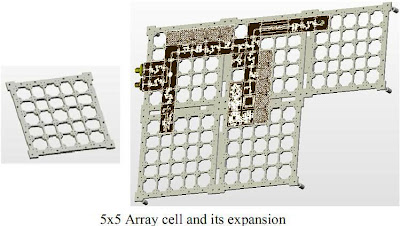
For the customer's easy integration and low cost consideration, MicroWaveCells also offers a 5x5 array mechanical cell; with the array joint cell, customers can build a very large system in a very short amount of time.


RF-Microwave Circuits/Microwave Circuits Prototyping and integration Revolution
fuente:http://www.microwavecells.com/ApplicationDetails/Prototyping.pdf
CRF_Zambrano C. Jaydi D.

RF-Microwave Circuits/Simulation Tools


Xpedion GoldenGate includes advanced RF and microwave simulators- RFlinear, RF non-linear harmonic balance with Krylov sub-space and envelope transient withnon-linear phase noise. Seamlessly integrated into widely used Affirma Analog Artist EDA environment, GoldenGate is complementary to Spectre RF and significantlyreduces design-cycles and design-time for wireless integrated circuits and products.

Today's wireless design teams require accurate and fast RF, microwaveand transient simulators to handle large and complex RFdesigns. There are stringent specifications for non-linearity, distortion, gain compression, harmonics, efficiency, phase noise and spurious mixing products. Circuits operate in highly non-linear and deep saturation regimes with digital modulated input signals. Also, RFintegrated circuits are tightly integrated with low frequency analog, DSPand digital designs. This requires the RFdesign environment to be tightly integrated with main stream EDA tools, to reduce the number of design iterations and design-cycle time. Xpedion GoldenGate is designed to meet the needs of wireless integrated circuit designers working in both defense and commercial wireless communications. It offers a set of the most sophisticated RF, microwave and envelope transient simulators combined with a unified set of accurate model libraries, complementary to Spectre RF. Simulators are optimized to handle today's 2G and 2.5G, evolving 3G,Bluetooth RF integrated circuits and complex modulation schemes. Users can perform multiple analyses, such as DC,multi-tone RF, and phase noise, all on a single schematic, while using various modulation sources.


Versatile analog, mixed signal and
RF/Microwave design environment

• Virtuoso Composer for entering hierarchical RF/Microwave and analog/mixed designs using GoldenGate and analog symbollibrary elements
• Fully customizable user interface with SKILL programming language
• Interactive GoldenGate circuit simulation allows quick design entry,change, analysis, display and manipulation of simulation results
• Schematic debug capabilities by cross referencing nodes, nets, and elements
• Industry standard EDIF interface

Devices and Libraries

• Ideal, linear, non-linear and lumped elements, extensive models for BJT,GaAsFET, MOSFET, JFET, diode
• Extensive, and accurate models for microstrip, stripline, coupled, coplanar,suspended and finline structures
• QAM, QPSK, pulse, Chirp, and user-defined modulation sources


Simulators / Analyses

• Three independent tones, unlimited number of harmonics
• Oscillator, amplifier powerup transient analysis, I/V vs time waveforms
• VCO, free running and locked oscillator, analog PLL, phase noise
• ACPR, NPR, SNR, BER, Eye diagram, constellation, EVM,AM/AM, AM/PM
• IP3, IP5, IM3, PAE, power, tone and noise spectrum, group delay
• S, Y, Z, H, noise parameters, VSWR, NF , NFmin, Sopt, Yopt,MAG, MSG
• DC, linear, non-linear Nyquist stability analysis, K factor, oscillator frequency
• DC I-V curves, load lines
• Yield and Monte Carlo analysis
• Eight choices of optimizers
• EM simulator interface using s-parameter files


Results Display

• GoldenGate uses Analog Artist's versatile results display tool
• Waveform calculator for extensive RF/Microwave results post-processing
• Smith chart, gain, noise figure circles,linear and log plot, load pull curves
• Nyquist stability circles
• Single and multiple Y-axes, line markers, pan and zoom, overlay plots from different simulations.

Other Related Products

• GoldenGate/Neural Net ModelCompiler generates accurate C-models for RF , microwave linear and non-linear circuits and discrete active and passive devices
• GoldenGate is interfaced with several system level simulators, including SystemView, SPW, and COSSAP
• GoldenGate is available on Windows 95, 98, NT, integrated with Orcad
• Import Spice models, mathematical sources and Spice circuit netlists.

RF-Microwave Circuits/Simulation Tools
fuente:http://www.cms-tech.co.kr/xpedion/pdf_files/GG_Sim_AA.pdf
CRF_Zambrano C. Jaydi D.

RF-Microwave Circuits/Design/Layout


RF-Microwave Circuits/Design/Layout
fuente:http://www.jlab.org/accel/eecad/pdf/050rfdesign.pdf
CRF_Zambrano C. Jaydi D.